|
|
Your source of photonics CAD tools | |
|
| ||
CrystalWaveA powerful photonic crystal simulator |
    |
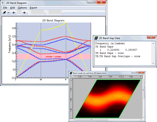
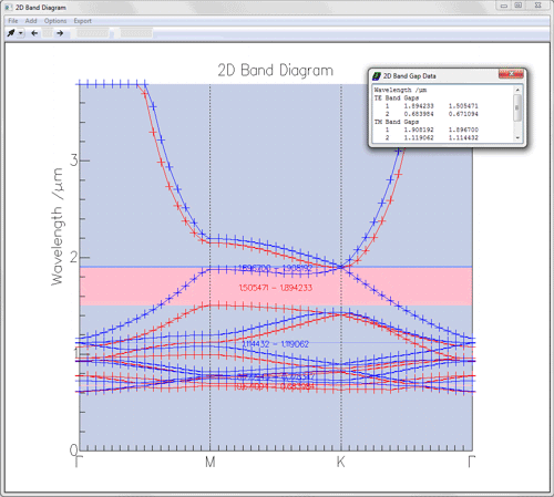
Band diagram of a 2D photonic crystal latticeSimulation with CrystalWave softwareCrystalWave can be used to design and simulate any kind of photonic crystal waveguide. In this case we are calculating the band diagram and identifying the photonic band gaps of an hexagonal 2D photonic crystal lattice by two methods: using CrystalWave's Band Structure Analyser and FDTD Engine.
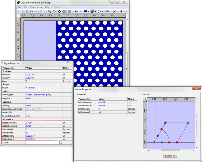
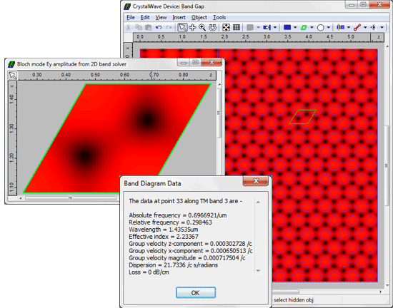
Design of the photonic crystal structureWith CrystalWave, designing and modifying a photonic crystal lattice is extremely easy. CrystalWave's editor comes packed with dedicated tools to create and modify 2D and 3D photonic crystal lattices, introduce point and line defects and offset lattice atoms from their ideal positions (offsets can be randomised for tolerance studies). Atom can be defined using a set of 2D and 3D shapes (ellipses, polygons, ellipsoids) which can be coated with a defined thickness. In order to design the 2D hexagonal photonic crystal below, we simply added a lattice to shape (one click) and changed the lattice angle and constants to fit our requirements. The lattice itself was filled with circular atoms in a simple click. The lattice period was set to 0.4284um and the hole diameter to 0.25969um.
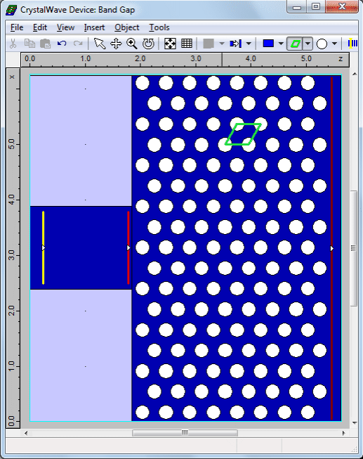
The optical properties of the different regions were defined for 2D simulations. In this case the dark blue areas have a refractive index of 3.2 whilst the white holes and the pale blue background have a refractive index of 1. The last step was to add a unit cell to the structure, in order to tell the Band Solver on which part of the device to perform the simulation. An input waveguide, an excitor and some sensors were also added to perform an FDTD simulation on the same structure.
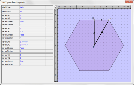
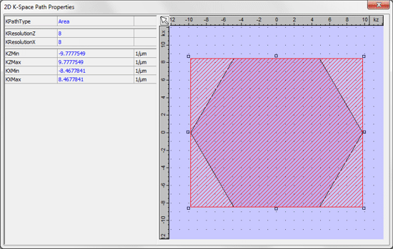
Calculating a band diagramThe band diagram was calculated with CrystalWave's Band Structure Analyser. The Brillouin zone was calculated and the irreducible Brillouin zone around which the calculation is performed was identified automatically; in this case the K-path is the conventional ΓKMΓ path used for hexagonal lattices. It can be inspected and modified by the user from the panel shown below.
The band diagram was calculated for TE and TM bands. The band diagram can be plotted against wavelength, absolute frequency or relative frequency; it is shown plotted against wavelength below. There is a large band gap for the TE polarisation between 1.505um and 1.894um.
The field profiles and properties of the Bloch mode at a given band point can be inspected; a TM Bloch mode is shown below along with its properties (wavelength, effective index, group index, dispersion, mode loss etc.).
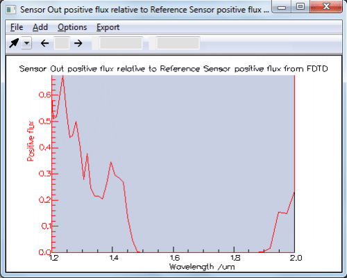
The results were checked with an FDTD simulation. A sinusoidal pulse of light centred on a wavelength of 1.55um was launched from the excitor and a spectrum of the transmission through the photonic crystal region was generated. As expected, it shows that no light is transmitted for the wavelengths in the photonic crystal band gap, between 1.5 and 1.9um.
Band diagrams of 2D lattices and 3D lattices can also be calculated in 3D. Calculating band surface and equi-frequency contoursIt is also possible to use the Band Structure Analyser to perform a band calculation over an area of the K-space. This will allow you to calculate the band surfaces and generate plots of the equi-frequency contours, as shown below.
An example of band surface is shown below.
|

 © 2023 Photon Design copyright all rights reserved |

 |