CrystalWaveA powerful photonic crystal simulator |
    |
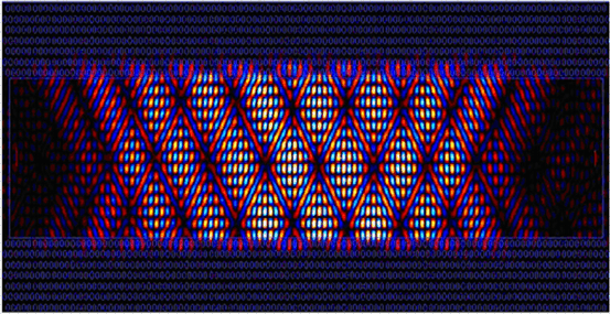
Photonic Crystal LasersSimulation of photonic crystal lasers with CrystalWave's Active FDTD softwareCrystalWave's Active FDTD module can be used to model photonic crystal lasers (PC lasers) and other nano-cavity lasers realistically. It can be used to model laser geometries that could not be simulated with conventional laser diode models. You can see for instance in the picture below the field profile distribution of a Littrow mode inside a photonic crystal laser cavity simulated in CrystalWave.
The Active FDTD module supports two different gain models:
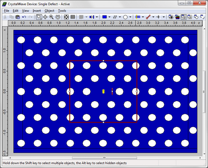
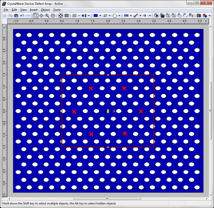
Modelling a photonic crystal laser cavityWe used CrystalWave to reproduce the results given in [1] for various geometries of photonic crystal laser cavities. We consider two designs: a cavity formed by a single lattice defect, and a larger cavity formed by a combination of seven lattice defects placed at the vertices and in the centre of an hexagon. As we will show below, the array of defects will allow us to obtain a higher laser output and a better defined farfield. The photonic crystal is etched in a thin membrane of active material (InP); the membrane is 280nm thick and surrounded by air on both sides. We create resonant cavities in the membrane by removing single holes; the resonant frequencies can be determined using a standard FDTD calculation without the gain present. For the single-defect structure, we find a resonant wavelength of 1.25μm.
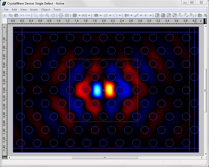
Simulation results: single cavityWe simulated both designs using the Active FDTD Engine with the Static Gain model, with a grid of 20nm and a duration of 7ps; the steady-state was reached after 2ps. You can see below a screenshot of the Hy field for the resonant mode of the single cavity.
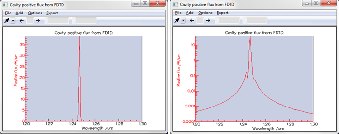
This is a measurement of the resonant spectrum after 7ps. It shows a single peak at 1.246um with a very narrow linewidth of the order of 1nm.
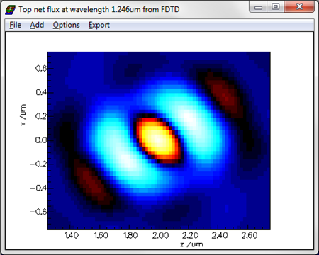
You can see below a map of the net flux above the membrane at the main resonant wavelength. The profile lacks the symmetry of the structure since the hexagonal structure has 3-fold symmetry leading to degenerate modes.
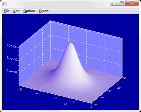
We placed a sensor on top of the cavity and calculated the farfield of the radiation emitted at the resonant wavelength, plotted versus lateral position. The farfield reveals that the single cavity does not provide a directional beam: measuring the FWHM of the profile reveals a horizontal half-angle of 55 degrees and a vertical half-angle of 27 degrees.
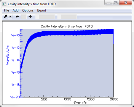
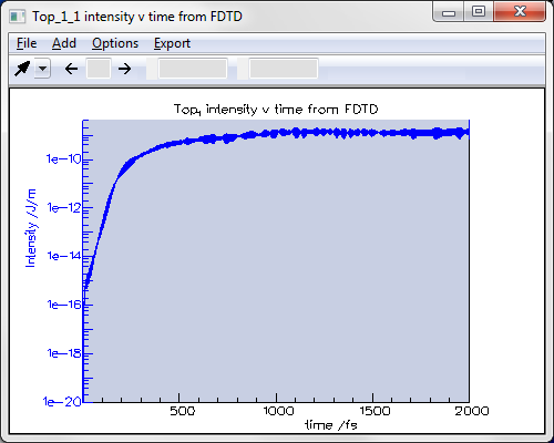
Using an FDTD Engine allows you to study the dynamics of your laser. You can see the evolution versus time of the intensity emitted by the cavity during the transitional regime, plotted below in log scale; at t = 0 a low-power pulse was emitted by a dipole in the centre of the cavity.
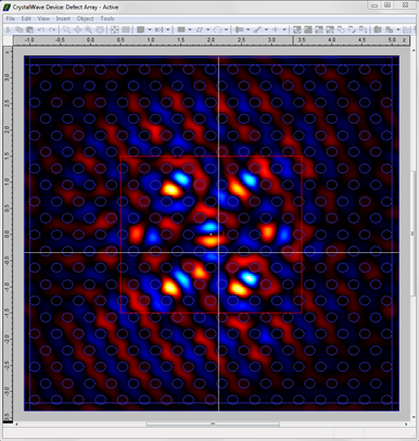
Simulation results: cavity arrayWe performed a similar calculation with the cavity array. You can see a screenshot of the resonant supermode below.
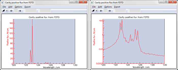
You can see below the spectrum of the resonance measured in the centre of the cavity array, plotted in linear (left) and log scale (right). The combination of the cavities leads to a splitting of the resonance peak, due to the presence of the cavity supermodes. The dominant peak after 7ps is the resonance at 1.231um, which corresponds to the lasing mode. This resonance has a linewidth of the order of 0.3nm.
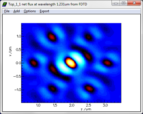
You can see below a map of the net flux through a plane distant from the membrane at the wavelength of the laser.
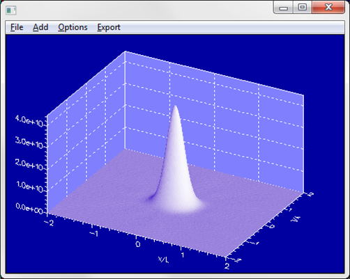
We plotted the wavelength and found a much narrower farfield profile than for the single cavity, with a horizontal half-angle of 22 degrees and a vertical half-angle of 12 degrees.
You can see below the evolution versus time of the intensity emitted by the cavity during the transitional regime, plotted in log scale.
ConclusionsThe Static Gain model of OmniSim and CrystalWave’s Active FDTD module was used to simulate two different designs of photonic crystal lasers; we were able to characterise the field distribution and the farfield associated with each laser, as well as the spectrum of the light inside the nano-cavity. ReferencesW. H. P. Pernice, F. P. Payne and D. F. G. Gallagher, J. of Light. Tech., 25, 9, pp. 2306-2314 (2007)
|

