FIMMPROPA bi-directional optical propagation tool |
   |
A Planar Silicon MMI Wavelength Demultiplexer3D simulation with FIMMPROP softwareWe used FIMMPROP to simulate in 3D a 1.3um / 1.55um wavelength splitter based on a 1x2 MMI design fabricated in SOI. The simulated device is adapted from the structure presented in [1]. Benefits of using FIMMPROP to model MMI couplersEME (EigenMode Expansion) is the ideal method to model MMI couplers. The physics of MMIs results from constructive and destructive interferences between a small number of guided modes; it is these interferences that give MMIs their ability to generate multiple images of the input beam. EME is a mode-based approach, and it therefore offers an extremely efficient way of modelling such devices. The implementation of EME in FIMMPROP offers an optimal framework for this application, with a potential for highly efficient optimisation and fully vectorial solutions:
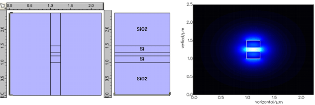
Design of a SOI MMI wavelength demultiplexer Design of a SOI MMI wavelength demultiplexerThe principle of the MMI wavelength demultiplexer is simple: the two injected wavelengths will have different beat lengths in the MMI section, generating self-images at different positions. In order to couple each wavelength to one of the output channels, the length of the central section was optimised to be an odd multiple of the beat length of the MMI for the wavelength of 1.3um (anti-symmetric self-imaging) and an even multiple of the beat length of the MMI for the wavelength of 1.55um (symmetric self-imaging). The design relied on a slot waveguide cross-section, in which the field is confined in a low-index layer located between two silicon layers embedded in a silica cladding. The modes of this waveguide were calculated with the FDM Solver.
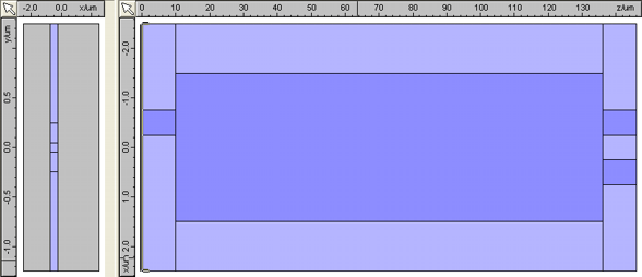
The input waveguide was shifted from the centre of the structure by 1/6th of the full width of the MMI, and the output waveguides were located at +/- 1/6th of the full width. A diagram of the full device and the full list of parameters is shown below. The dimensions of the structure are the ones described in [1], except for the width of the input and output waveguides which was set to 0.5um.
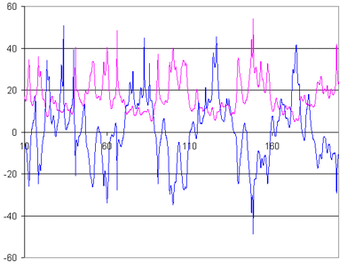
Performance optimisationThe device was optimised by scanning the length of the multimode section and calculating the power in each output branch at the wavelengths of 1.3um and 1.55um. FIMMPROP relying on EME, the length of a section of the device can be changed at a minimal cost in calculations and time. Simulating the MMI coupler at one wavelength with FIMMPROP took 2 minutes and 40 seconds with an Intel Pentium 4 CPU running at 3GHz, with 40 modes included in the multimode section. Once the MMI coupler simulated, obtaining the evolution of transmission when scanning the length of the multimode section over 200 values only took 3 seconds! This allowed us to optimise the device very efficiently and with an extremely fine resolution! Below is plotted the evolution of the contrast and insertion losses for varying length of the central section of the MMI. The contrast at a given wavelength is defined by the ratio in dB of the power in the two output channels, defined in such a way that it must be maximised. The insertion loss is the ratio in dB of the output power by the input power, which has to be minimised.
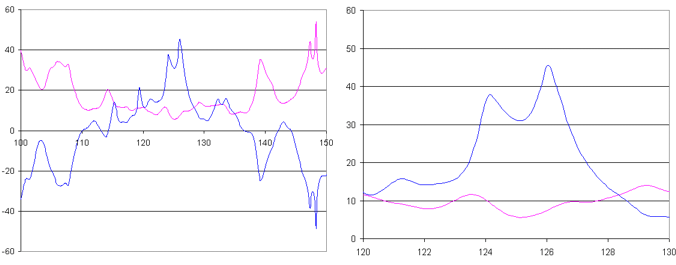
Running the scanner over a large range of MMI length allowed us to identify multiple optima (for lengths of 33.47um, 82.36um, 126.06um, 174.49um), which offered different possibilities of design. An optimum will be more interesting than another depending on whether you want to obtain maximum transmission, or minimum unwanted cross-coupling, or similar coupling coefficients at both wavelengths etc. Optimal design investigationThe maximum contrast for minimal cross-coupling was obtained for a length of 126um, as can be seen in the graphs below.
This allowed us to obtain the following performances:
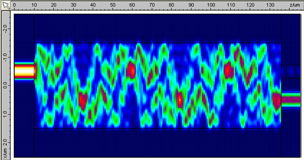
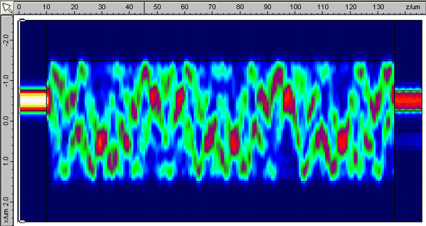
FIMMPROP can easily plot intensity profiles, shown below for wavelengths of 1.3 and 1.55um.
Reference[1] Jinbiao Xiao, Xu Liu, and Xiaohan Sun, "Design of an ultracompact MMI wavelength demultiplexer in slot waveguide structures," Opt. Express 15, 8300-8308 (2007)
|

