|
|
Your source of photonics CAD tools | |
|
| ||
FIMMPROPA bi-directional optical propagation tool |
   |
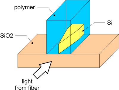
An Inverted Optical Taper (Fiber to Chip Coupler)3D simulation with FIMMPROP softwareFIMMPROP was used to simulate an example of inverted optical taper presented in [1], in which a silicon nanowire is laterally tapered whilst enclosed in a larger cladding of high-index polymer. FIMMPROP was able to model this structure with a precision of 0.1% in 17s on a standard desktop computer (full vectorial 3D). It was then able to scan the length of the taper instantly. A well-known challenge for silicon photonics is to obtain efficient coupling between the highly confined mode in an integrated optical waveguide or a photonic integrated circuit (PIC) and the large-diameter mode in the optical fiber used to couple light in and out of the chip. Due to the large mismatch between the mode sizes and effective indices, direct coupling would result in dramatic losses. Several solutions have been proposed to overcome this challenge, which include the use of surface gratings and tapers in which both the thickness and the width of the silicon layer are increased. However, inverted lateral tapers offer a much simpler approach in terms of fabrication process. In an inverted lateral taper, the silicon layer is embedded in a larger cladding of intermediate index e.g. SiN or a high-index polymer. As the width of the silicon core is tapered below cut-off, the mode that was initially confined in the silicon core is converted into a much larger mode, now confined within the SiN or polymer cladding.
Why use FIMMPROP for this simulation?FIMMPROP is a very efficient tool for the simulation and modelling of optical tapers:
Taper DesignThe simulated structure is described in details in [1], and is pictured below. A silicon nanowire is placed on top of a silica substrate and embedded in a polymer cladding. The width of the silicon core is tapered linearly. The very small size of the silicon waveguide at the tip allows the mode to expand entirely in the polymer cladding, which acts as a secondary core. The size of the polymer cladding was chosen to obtain a maximum mode overlap with the mode of the SMF fiber used to inject and retrieve light from the structure.
The dimensions of the structure are summarised in
the table below.
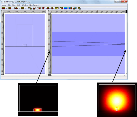
Taper ModellingThe taper was designed and simulated in 3D with FIMMPROP, the local modes being calculated with the non-uniform finite-difference FDM Solver.
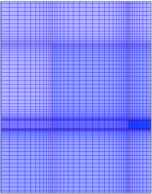
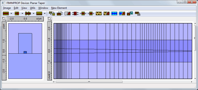
You can see the mesh used by the FDM Solver below; note how the mesh is refined at the interfaces between the materials, where the fields will vary more rapidly.
The taper algorithm relies on an adaptive z-step: as it starts discretising the structure, it will study the evolution of the modes along the z-axis and refine the discretisation selectively and dynamically. You can see the discretisation steps as black lines in the picture below; note that the discretisation is much finer at the beginning. To obtain the same level of accuracy with a uniform z-step, you would need a much larger number of steps!
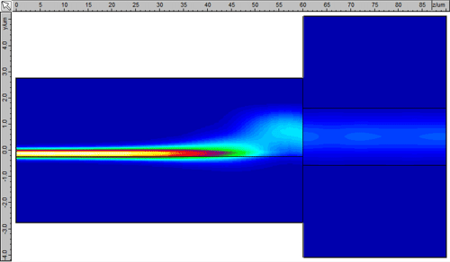
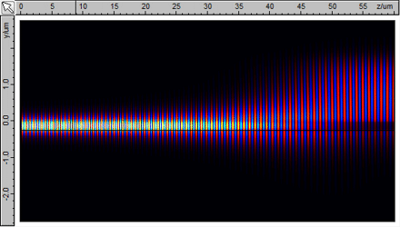
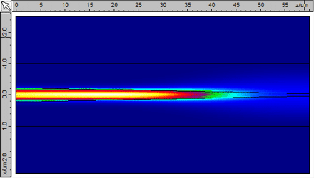
The combination of non-uniform mesh, adaptive z-discretisation and solver specific overlap calculations allows us to model the taper with a precision of 0.1% in just 17 seconds on a 4-core i7-2600 CPU. Simulation ResultsThe evolution of the intensity profile along the taper is plotted below. The transition between two confined states can be clearly seen in the last third of the taper.
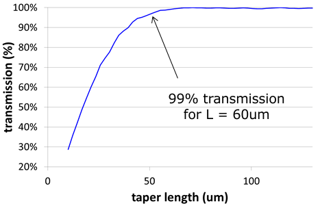
FIMMPROP allows you to vary parameters in order to optimise your design very efficiently. For instance, whilst the calculation of the taper itself took 17s, scanning the length of the taper only takes a fraction of this time and a scan of 128 points was obtained in 2.5 seconds! This allowed us to plot the study the evolution of transmission with taper length, which is shown in the figure below. This reveals that an adiabatic taper can be obtained for a taper length as small as 60um (99% transmission).
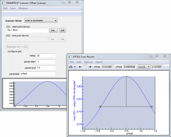
The matching between the fiber and the chip was optimised by varying the vertical alignment using another FIMMPROP Scanner. The results are shown below.
Reference[1] S. J. McNab, N. Moll and Y. Vlasov, "Ultra-low loss photonic integrated circuit with membrane-type photonic crystal waveguides", Optics Express 11, 22, p. 2927-2939 (2003)
|
 © 2023 Photon Design copyright all rights reserved |

 |