|
|
Your source of photonics CAD tools | |
|
| ||
PICWaveA photonic IC, laser diode and SOA simulator |
    |
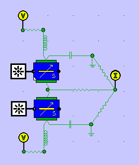
Balanced photo-detector / photodiodesSimulation with PICWave softwareIn PICWave, arbitrary LCR networks can be constructed and attached to active sections. This example shows a balanced photo-detector, which measures the difference (in the form of an RF output voltage) between two optical input signals. The balanced photo-detector circuit, shown below, consists of two photo-diodes coupled together with an electrical network, which acts to amplify the difference between the electrical responses of the photo-diodes, but not the particular responses of each. A constant bias is applied across the two photo-diodes using two voltage drives and the RF output voltage is measured using a current drive (injecting 0 Amps) which has a built-in voltage instrument.
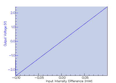
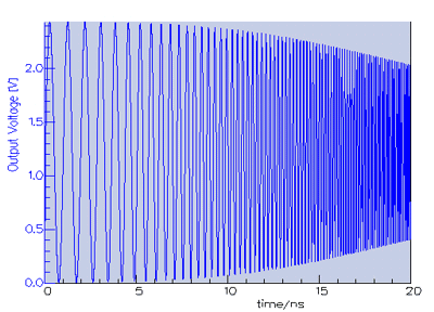
The figure below shows the DC and AC response of the balanced photo-detector.
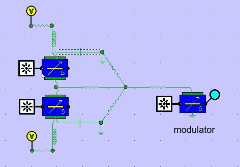
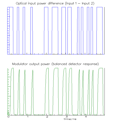
You can see below a new circuit in which the balanced photo-detector is used to drive an optical modulator, in which a CW signal is injected.
You can see below the juxtaposition of the evolution with time of the difference in optical power between the two photo-diodes and of the output power of the modulator. You can observe how the signals are matched.
|
 © 2023 Photon Design copyright all rights reserved |

 |