CrystalWaveA powerful photonic crystal simulator |
    |
A Photonic Crystal Waveguide Y-junctionFDTD simulation with CrystalWave softwareCrystalWave can be used to design and simulate any kind of photonic crystal waveguide. In this case we are modelling an hexagonal 2D photonic crystal lattice in which a Y-junction waveguide is created by introducing line defects. Design of the photonic crystal waveguideWith CrystalWave, designing and modifying a photonic crystal lattice is extremely easy. CrystalWave's editor comes packed with dedicated tools to create and modify 2D and 3D photonic crystal lattices, introduce point and line defects and offset lattice atoms from their ideal positions (offsets can be randomised for tolerance studies). Atom can be defined using a set of 2D and 3D shapes (ellipses, polygons, ellipsoids) which can be coated with a defined thickness.
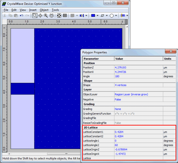
In order to design the Y-junction below, we simply added a lattice to shape (one click), changed the lattice angle and constants to fit our requirements.
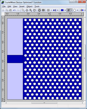
We then automatically filled the lattice with 2D circular atoms.
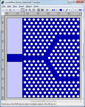
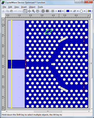
Using the "line defect" tool, which allows you to remove or add a line of lattice atoms, we created the Y-junction. The two pictures below show the device before and after the addition of line defects. Only one click was needed to create each segment!
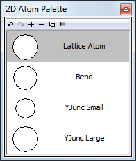
The next stage is to add the individual atoms to optimise the transmission, as well as the excitor (yellow line) and the sensors (red lines) to inject and measure the field. The position of the individual non-lattice atoms was optimised using our optimisation tool Kallistos.
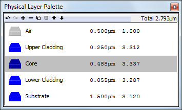
Definition of the materials and optical propertiesWe have then set up the optical properties of the different regions of the structure for 2D and 3D calculations. CrystalWave allows you to perform 2D and 3D calculations on the same structure. For 2D calculations, each colour on the layout is associated with a given material. In this case the refractive index of the dark blue region was set to 3.2 whilst the white holes and the pale blue background were set to air. The 3D structure is designed as follows: we start by defining an epitaxial structure along the vertical direction, which is grown throughout the device. This structure is then modified by defining masks for the "etch", "fill" and "grow" operations that you would use to create your physical structure. In this case we will grow the epitaxial structure shown below in the whole device and then etch the pale blue background region and the atoms, which will be filled with air.
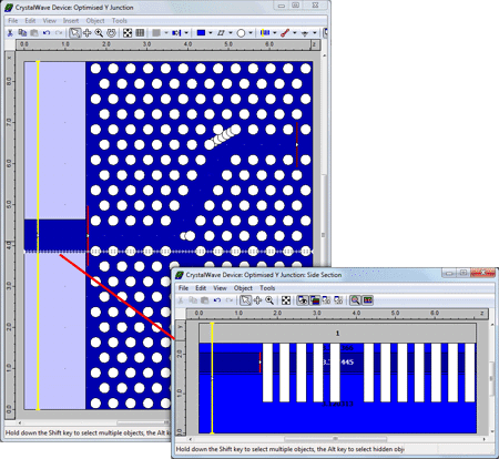
Note that the same shapes and atoms are used to design the 2D and the 3D structures, allowing you to easily set up both at the same time! This will allow you to perform a quick 2D calculation to check your design before running a more time-consuming 3D calculation. You can inspect the structure in 3D using cross-section views, as shown in the picture below. In this case, you can see that the atom layers are only extending from the top of the structure to the middle of the of the substrate layer.
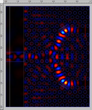
Simulating the structure with CrystalWave's FDTD EngineThe structure was simulated with CrystalWave's 2D and 3D FDTD Engine. You can run the video below for a live recording of the 2D FDTD calculation: Calculating the relative flux in each sensor reveals that 95% of the input power is coupled to the two branches, showing an excellent transmission. |

