|
Introduction
Features
‣
Layout Editor
‣
FDTD Engine
‣
Cluster for FDTD
‣
Active FDTD
‣
FETD Engine
‣
FEFD Engine
‣
RCWA Engine
‣
Band
Structure
Analyser
‣
Scripting / Optimisation
‣
GDSII Export
Applications
Options
Publications
Download Brochure
Request evaluation
|
Layout Editor
A mask layout editor optimised for photonic crystal
structures
CrystalWave provides probably the most powerful, user-friendly graphical user interface for the design of photonic crystals available on the market today.
For the planar integrated photonics please see
also the
OmniSim Editor (available as part of CrystalWave).

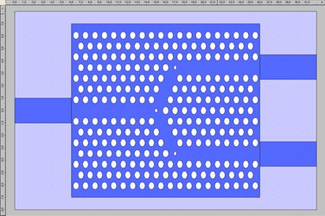
A photonic crystal Y-junction designed in CrystalWave
You can use the mouse to lay out atoms
in lattices, point and line defects, quickly and as easily as using a
common drawing package; creating with ease even the largest of
structures with tens of thousands of atoms.
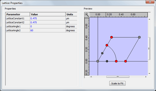
Numerical input allows fine control of lattice parameters and atom positions, shapes and sizes. You can also use the script system to fully automate the construction of even the most complex structures.
Features:
2D and 3D photonic crystal lattices Hexagonal, rectangular and any other regular lattices User may specify lattice vector directions and lattice
constants Atoms may be circular, elliptical, rectangular, regular or irregular polygons Easy to change the positions, shapes and sizes of large numbers of atoms Easy to place single and line defects
-
Individual atoms may be offset from their lattice points in both 2D and 3D lattices
Multiple crystals, e.g. one region with lattice vectors at 0° and 60° and another with vectors at 5° and 65°
Device layer editor for quick definition of your epitaxial structure Supports etch and growth processes Advanced etch process:
Free rotation of any object Definition of conventional waveguides into the lattice Multi-level undo/redo
-
Constraint system to build complex structures by joining elements together
Export to mask file with advanced mask generation features

Defining the properties of your 2D lattice
|


