|
Introduction
Features
‣
Layout Editor
‣
FDTD Engine
‣
Cluster for FDTD
‣
Active FDTD
‣
FETD Engine
‣
FEFD Engine
‣
RCWA Engine
‣
Band
Structure
Analyser
‣
Scripting / Optimisation
‣
GDSII Export
Applications
Options
Publications
Download Brochure
Request evaluation
|
Band Structure Analyser
CrystalWave offers a Band Structure
Analyser relying on plane-wave expansion (PWE) as an optional module.
This tool will allow you to
calculate the band diagrams and band surfaces (contours of
equifrequency) of arbitrary photonic crystals in 2D and 3D. It can also
be used to calculate Bloch
modes, for instance in a line defect operating as a waveguide.

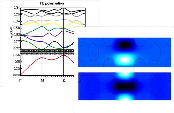
Band Structure Analyser: band diagram and Bloch modes of a line defect.
The two plots are of the same Bloch mode with a half-period difference.
The analysis of the band structure of a
periodic lattice is a very useful starting point for a photonic crystal
circuit design. In essence it computes the solutions of a structure with
infinite periodicity. This can be a "bulk" lattice but could also be a
line defect, telling you when the lattice is opaque, when a line defect
supports a single mode and so on.
The Band Structure Analyser will compute the Bloch (periodic) modes of a photonic crystal lattice with 2 or 3 dimensional periodicity. It will automatically identify the band gaps of your structure and evaluate the Bloch mode profiles at any point.
Features of the band structure
analyser:
- PWE (plane wave expansion) based engine for best computation in the frequency domain.
Much faster than FDTD-based band solving methods.
- 2D and 3D simulation modes; in 3D you can simulate both
2D and 3D lattices.
- Generates w/k band diagrams for TE-like and TM-like polarisations.
- Band surface calculations for the Brillouin-zone and equi-frequency contour plots.
- Easily plot the Bloch modes from any point on the w/k
band diagram.
- Full integration with the CrystalWave framework.
- Simple graphical specification of Cartesian and
non-Cartesian unit cells.
- Supports all lattices definable in the CrystalWave layout
editor - rectangular, hexagonal lattices, with square, elliptical or
arbitrary shaped "atoms".
- Automatic detection of band gaps.
- Add light lines to your band diagrams in one click.
- Real and lossy materials.
- Calculate effective index, group index and dispersion of
the Bloch mode.
- Automatic scanners for generation of "band maps" e.g.
against lattice period or hole size.
- Speed optimised calculation engine takes advantage of any
symmetries.

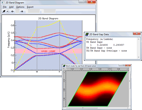
Band diagram of a 2D lattice with band gaps, light line and Bloch mode
profile

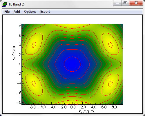
Band surface plot for a 2D hexagonal lattice
showing the equi-frequency contours.
|


