|
|
Your source of photonics CAD tools | |
|
| ||
OmniSimOmni-directional photonic simulations |
    |
Optimisation of Silicon Nanophotonic DevicesSimulation with OmniSim FEFD software and KallistosKallistos was used to optimise light transmission through two silicon nanowire devices, which were defined and simulated in OmniSim with the FEFD Engine:
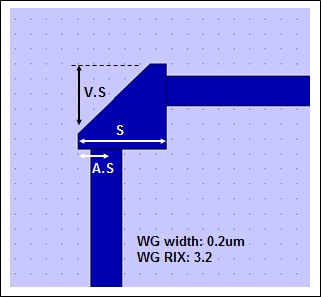
Optimisation of a 90 degree silicon waveguide cornerWaveguide bends are basic structures for optical interconnects and therefore very important components in optical integrated circuits. Any abrupt directional change in dielectric waveguides causes a rotation of the phase fronts of the propagating modes. This perturbation causes mode conversion into unguided modes giving rise to radiation loss, mostly at the outer side of the corner. In this case, we attempt to improve the performance of a 90-degree sharp bend by placing a resonant cavity at the corner, capable of steering the waveguide mode with very low radiation loss. This could be achieved by placing a quarter-disk at the corner as a curved Fabry–Perot resonator, however it is desirable to avoid curved interfaces that are harder to fabricate. Instead the corner was created by making a 45-degree cut at the outer corner of the square. In this configuration the strongly guided waveguide mode undergoes total internal reflection at the 45-degree cut and is guided around the modified corner by the outer walls. The structure is shown below. Light is injected from the bottom of the device and the transmission is measured at the right hand side.
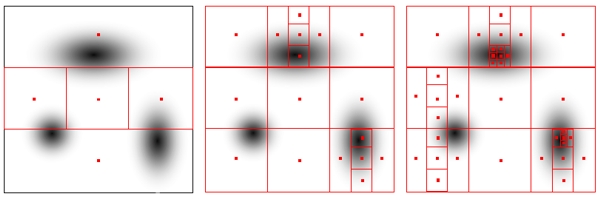
Three parameters were modified by the optimiser: the size of the resonator box "S", the relative position of the slant "V" and the relative position of the waveguides "A". The Deterministic Global OptimiserKallistos' deterministic Global Optimiser was used to optimise the structure. This algorithm systematically searches the parameter space and successively subdivide regions in systematic way. This guarantees that the global optimum is found if the optimiser is run for long enough, even if multiple local optima exist. This is illustrated in the figure below, which shows the calculated data in a 2-parameter space at various stages of the optimisation; the dark areas correspond to the local optima. You can see that the algorithm divides more quickly where optima are “more likely” to exist.
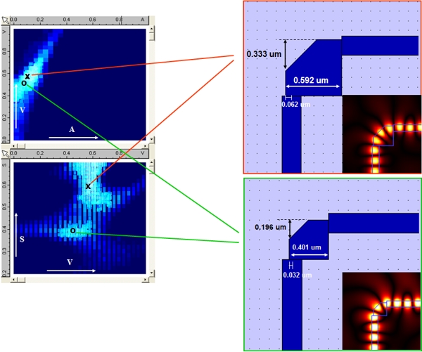
Optimisation resultsThe results of the optimisation are shown below. On the right hand side, you can see two 2D maps of the parameter space: (A, V) at the top and (V, S) at the bottom. The optimisation data is represented using a colour scheme in which the optimal solutions are shown in white and the worse solutions in dark blue. Kallistos allows the user to choose among several devices of equivalent performance. In this case, you can see on the bottom map that there are two distinct global optima "O" and "X", for which respective transmissions of 98% and 99% is obtained (±1%). The optimiser provides you with information about the performance of the device around each optimum, allowing you to take the fabrication tolerance into account when choosing the optimal design! In this case the main difference between the two solutions is the size of the resonator "S". The corresponding devices are shown on the left-hand side, "X" at the top and "O" at the bottom, and the field profile corresponding to light propagation through the corner is shown in insert of each device. The field plots reveal that optimal transmission is achieved when the size resonant box matches an integer number of half oscillations of the field (3 half oscillations for "X" and 2 half oscillations for "O").
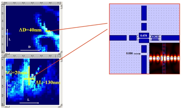
Optimisation of a 90 degree silicon waveguide crossingWaveguide crossings are important components of an optical integrated circuit as they allow the interaction of many waveguides within a limited space. Ideally the wave launched in one of the intersecting waveguides must be fully transmitted forward without any power escaping sideways (no crosstalk) and with negligible reflection and radiation loss. This can be obtained by introducing a resonant cavity at the centre of the intersection. In this example, we attempt to optimise the structure by introducing a resonator box in the centre of the crossing, and two gaps in each of the waveguides leading to and from the resonator, one of them directly after the resonator. The structure is shown below.
The same optimisation method was applied to this design. Three parameters were modified by the optimiser: the size of the resonator box "D", the length of the discontinuity "L" and the gap size "G". Optimisation resultsThe results of the optimisation are shown below. On the right hand side, you can see two 2D maps of the parameter space: (D, L) at the top and (L, G) at the bottom. The optimisation data is represented using a colour scheme in which the optimal solutions are shown in white and the worse solutions in dark blue. In this case, a single optimum is found, giving 99% power transmission (±1%). Inspection of the optimisation maps gives an indication of the sensitivity of the optimal transmission to parameter variations. The optimum shape is found for D=0.478 um, L = 0.263 um, G=0.056 um, but the optimiser reveals that the transmission will remain above 97% when G varies between 0.04um and 0.08um, L between 0.20um and 0.30um, and D between 0.46um and 0.52um.
ReferenceT. P. Felici, D. F. G. Gallagher, Lorenzo Bolla, "Automatic Design and Optimisation of Si nanophotonics devices using Finite Element Frequency Domain Solvers", Proc. SPIE, Vol. 4986, p.375-385 (2003)
|

 © 2023 Photon Design copyright all rights reserved |

 |